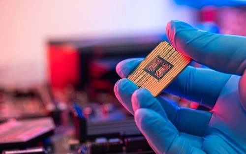
Executive summary

For nearly three decades, physical design followed a familiar rhythm as transistors shrank, tools improved, and engineers learned new rules while the underlying game stayed fundamentally the same. Close timing, fix congestion, strengthen the power grid, tape out. That rhythm has now broken at 3 nanometer and below, where physical design is no longer a downstream execution problem but has become a system-level orchestration challenge in which device physics, interconnect behavior, power delivery, packaging, and AI-driven automation interact in ways that defy the mental models we built over previous generations. Engineers are no longer just closing layouts but shaping how silicon systems behave across multiple dies, package layers, and thermal boundaries. TSMC began volume production of its N2 node in the second half of 2025 with nanosheet gate-all-around transistors, while Intel’s 18A combines RibbonFET gate-all-around devices with PowerVia backside power delivery in the industry’s first production deployment of power routing underneath the transistor layer. We still achieve density improvements approaching 20 to 25 times from 28-nanometer to current 2-nanometer-class processes, yet extracting these gains demands exponentially more sophisticated implementation strategies.
Physical design (PD) teams no longer execute sequential flows. We now manage multi-physics optimization problems where dynamic IR drop shifts path delays, backside power via pillars constrains placement density in ways coupling directly to supply resistance, chiplet-to-chiplet latency budgets shape floorplans across multiple dies, and reinforcement learning agents explore design spaces exceeding human evaluation capability. My team closed designs at 28 nanometer by optimizing wirelength and managing a few hundred timing corners. Today at 3 nanometer, engineers must understand waveform-dependent delay models, spatial correlation in IR variation, color-aware routing constraints, nanosheet width selection, and how to guide machine learning systems. This article explores three forces driving this transformation through advanced process nodes, introducing gate-all-around devices and backside power delivery, chiplet-based and 3D integration moving system architecture inside the package, and AI becoming embedded within physical design flows. Together, they are redefining how we design chips and who the physical design engineer must become. Organizations treating physical design as a back-end implementation task will struggle, while those recognizing PD has evolved into a system-level discipline requiring cross-functional expertise will define what becomes possible over the next decade.
Why gate-all-around transistors forced methodology changes
Samsung moved to gate-all-around transistors at 3 nanometer in 2022, while TSMC extended FinFET architecture to 3 nanometer before transitioning to GAAFETs at 2 nanometer. FinFETs delivered strong scaling from 22 nanometer through 7 nanometer and maintained viability even at 5 nanometer, but approaching 3 nanometer dimensions exposed fundamental limitations in how well a tri-gate structure could control current flow through increasingly short channels. Engineers adjusted fin heights, modified fin widths, and explored various geometry tweaks, yet leakage currents and short-channel effects refused to improve proportionally to the area reductions being achieved. Surrounding three sides of a vertical silicon fin could not provide sufficient electrostatic control once channel lengths dropped below certain thresholds.
Gate-all-around nanosheet transistors solve this by wrapping the gate electrode completely around horizontally stacked silicon channels. TSMC brands this approach as nanosheet technology within its N2 family, offering NanoFlex capability that allows designers to mix different sheet widths and counts within the same design. Stronger electrostatic control translates directly to lower leakage and improved subthreshold slope, while better current drive enables more granular performance versus leakage trade-offs at the cell level. Sheet width becomes an additional tuning parameter beyond threshold voltage selection, giving physical design teams another optimization axis for block-level PPA goals.
The device roadmap stopped being a background context that implementation teams could ignore. Cell library selection evolved from a project kick-off decision into an ongoing optimization variable, with different design regions benefiting from different sheet configurations depending on local timing criticality, power density, and congestion characteristics. When I discuss these transitions with engineering teams making their first advanced node tape-outs, a consistent pattern emerges. The initial assumption treats GAAFETs as improved FinFETs that should integrate into existing flows with minimal methodology changes. Reality surfaces during silicon bring-up when unexpected variations in nanosheet selection or localized placement density create measurable shifts in delay distributions, leakage profiles, or aging behavior that signoff models failed to predict. Gate-all-around transistors addressed the electrostatic control problem, but device architecture alone could not solve the escalating power delivery challenges that would emerge at 2 nanometer and beyond.
How backside power delivery reshapes floorplanning constraints

Intel’s 18A node entered production readiness in 2025 as the industry’s first volume process combining gate-all-around transistors with backside power delivery through its PowerVia technology, TSMC’s N2P variant, incorporating backside power is expected in 2026. Relocating VDD and VSS rails underneath the device layer instead of sharing frontside metal tracks with signal routing should improve routability, reduce IR drop through shorter current paths, and lower overall PDN (Power Delivery Network) resistance. Intel’s test chips using PowerVia demonstrated greater than 90 percent cell utilization, more than 30 percent platform voltage droop improvement, and 6 percent frequency benefit compared to conventional frontside power delivery. The challenge for physical design teams is that backside power fundamentally reshapes implementation constraints in ways that propagate from floorplanning through placement, routing, and signoff.
Backside power structures require dense arrays of nano-TSVs (through-silicon vias) connecting transistors to power rails underneath the silicon layer. These vertical vias occupy area, impose alignment requirements, and create keep-out zones that interact with macro placement, standard cell density, and channel planning decisions. High-current regions concentrating switching activity now couple to local via pillar density in ways creating spatial variation in effective supply resistance. Floorplans failing to anticipate these interactions early will discover during placement that certain regions lack sufficient via density to support dynamic current demands without excessive droop, yet modifying via pillar distributions after placement requires disruptive rework since the backside structure ties directly to device-level layout.
PDN analysis transforms from primarily modeling 2D metal strap networks to full 3D simulation of vertical current flow through backside metals, nano-TSVs penetrating the silicon layer, and lateral distribution at the device level. Early production experience indicates that achieving convergent signoff demands significantly more iteration between floorplanning, placement, PDN synthesis, and extraction compared to previous nodes, with teams needing to model power delivery characteristics much earlier in the planning phase instead of treating PDN as a post-placement optimization problem.
Why advanced nodes deliver better transistors but harder closures

TSMC’s published specifications for N2 compared to the N3E project show a 10 to 15 percent performance improvement at iso power and a 25 to 30 percent power reduction at iso performance. Intel claims 18A achieves up to 15 percent better performance per watt and approximately 30 percent higher density relative to Intel 3. These improvements matter for product competitiveness and justify the enormous capital investments required to deploy new process nodes, yet they create what I describe as the implementation paradox. Each node transition adds constraints and complexity faster than it adds performance margin, making designs harder to close even though the underlying transistors improve.
Voltage scaling stopped delivering proportional power reduction around 7 nanometer, forcing dynamic power improvements to come primarily from reduced capacitance through careful device and interconnect design. Power density climbs relentlessly as AI and compute-intensive workloads drive higher utilization, with localized hotspots exceeding 5 watts per square millimeter becoming increasingly common. DRC (design rule check) and DFM (design-for-manufacturing) rule decks have grown from thousands to tens of thousands of individual checks as multi-patterning techniques introduce layer-specific manufacturability constraints.
Traditional mental models for implementation methodology became unreliable at 2 nanometer as timing margins could no longer be managed through simple global derates applied uniformly. At 5 nanometer and especially at 3 nanometer, delays become waveform-dependent as dynamic IR drop distorts signal edges, Miller coupling modifies transition times, and transistor models expose second-order effects that older models never needed to represent because those effects contributed negligibly to total delay at larger geometries. Path delays can shift by tens of picoseconds within a single clock domain depending on vector-dependent supply droop patterns, requiring timing analysis to account for spatial and temporal correlation in IR behavior. Routing constraints exhibit non-linear scaling as congested regions resolvable through targeted ECOs at 28 nanometer represent design crises at 3 nanometer. The escalation stems from compounding restrictions, as color patterning limits which metal layers support specific routing directions, unidirectional track assignments eliminate flexibility, and forbidden via patterns close off escape routes that previously provided relief. These compounding constraints at advanced nodes drove the semiconductor industry to reconsider whether forcing every function onto a single monolithic die still made economic and technical sense.
Why chiplets force system-level floorplanning
Leading-edge wafer costs approaching 30,000 dollars per wafer at 2 nanometer forced the semiconductor industry to reconsider whether manufacturing every function on the most advanced node in one piece of silicon remained optimal. Defect densities making extremely large monolithic dies economically questionable reinforced this shift toward heterogeneous integration. AMD’s Epyc and Ryzen families demonstrated that heterogeneous integration delivers compelling advantages by placing small CPU chiplets on leading-edge nodes beside larger I/O dies built at mature nodes. The Universal Chiplet Interconnect Express standard, updated to 2.0 in 2024 provides specifications for die-to-die communication spanning 2D, 2.5D, and 3D configurations with bandwidth densities reaching terabytes per second per square millimeter for UCIe 3D hybrid bonding. Smaller dies mean higher yield since individual defects kill less silicon area, while process node selection becomes flexible with analog blocks remaining on mature nodes as compute logic moves to advanced nodes. The scope expands from optimizing a single die to orchestrating system-level integration across multiple dies, package substrates, interposer routing layers, and thermal management paths.
Floorplanning evolved from positioning macros on silicon to determining chiplet arrangement within packages, communication across bump interfaces, power distribution strategies, and collective heat dissipation through substrate and thermal interface materials. Bandwidth-critical links between CPU and HBM (High Bandwidth Memory) or between GPU and accelerators require joint optimization with on-die NoC (Network-on-Chip) topology since inter-chiplet path delays often exceed on-die interconnect delays and become the limiting factor for performance. Cross-die timing closure becomes a first-class signoff with an analysis modeling package for parasitics, supply noise correlation across separate dies, and thermal gradients affecting different chiplets differently. Thermal constraints emerge as system-level limiters as HBM stacks beyond 12 layers experience sharply rising internal resistance through vertical heat conduction, while 3D logic stacks risk thermal runaway on internal die surfaces that cannot reject heat efficiently.
When AI became necessary for closing advanced node designs
At 3 nanometer and below, even the most experienced physical design engineer cannot mentally model the complete solution space anymore. Placement density interactions with power distribution create thermal hotspots that shift timing margins, which then feedback to constrain placement decisions in multi-way dependencies involving billions of individual cell positions. Multi-corner multi-mode timing analysis generates millions of potential violations addressable through different ECO strategies, each with different ripple effects.
Reinforcement learning for placement optimization has moved from research demonstrations to production deployment. Synopsys DSO.ai has achieved hundreds of commercial tape-outs since its 2020 launch, with customers documenting PPA improvements exceeding 10 percent, turnaround time reductions of 3 to 10 times, and specific instances showing 15 percent cell area reduction with 5 percent die shrink. STMicroelectronics publicly stated that DSO.ai increased their PPA exploration productivity by more than 3 times while enabling implementation of a new Arm core exceeding power, performance, and area targets.
AI applications extend throughout the implementation flow beyond placement. Graph neural networks trained on historical designs predict high-resolution congestion before detailed placement, while density optimization uses models correlating local placement density with path-level sensitivity and IR-induced delay shifts. Critical net layer assignment uses deep learning to predict optimal routing locations for clocks and sensitive paths to minimize late-stage SI and EM failures, while ECO generation employs RL to propose buffer sizing, cell swaps, or layer promotions that improve local slack while predicting global impact. Machine learning enables IR drop prediction from early layout data and EM risk forecasting based on via patterns before final routing completes, collapsing weeks of iteration into hours.
What companies must build to succeed at 1 nanometer
Physical design is transforming into a multi-physics system-level discipline requiring fundamentally different organizational structures compared to what succeeded at previous nodes. Today’s PD engineers must evolve beyond traditional placement and routing expertise into AI-native, multi-physics system designers. Skillset requirements now encompass variation-aware timing methodologies, including AOCV, POCV, waveform-based static timing analysis, aging models, and IR-dependent delay calculations. Power integrity and thermal co-design become mandatory when working with 3D PDN structures, dynamic IR analysis, EM lifetime verification, and thermal gradient management across stacked dies. Chiplet and 3D integration capabilities must span interposer design, RDL routing, cross-die timing closure, and system-level power and signal integrity, while AI-driven flow development requires understanding how to guide reinforcement learning algorithms, build predictive models, and recognize when human expertise should override algorithmic recommendations.
Methodologies must shift from sequential flows toward concurrent multi-physics optimization with different analyses informing each other continuously throughout implementation. Early IR and thermal-aware floorplanning perform power delivery and thermal feasibility assessment before placement instead of discovering problems at signoff, while BSPDN-aware (Backside Power Delivery Network) implementation integrates vertical PDN constraints from project start, and AI-in-the-loop flows allow reinforcement learning agents to drive placement, routing, and ECO generation as human engineers supervise exploration. Teams must restructure around cross-functional squads spanning silicon process, package design, signal and power integrity, architecture, and RTL development, with new specialized roles emerging to bridge these domains. PD data scientists build machine learning models for congestion prediction and IR forecasting, while chiplet and 3D integration architects own cross-die timing closure and thermal management strategies, as AI flow engineers configure reinforcement learning loops and construct automation frameworks that orchestrate multi-tool workflows.
The hybrid model pairing humans with AI will define tape-out success at 1.4 nanometer and beyond, with human engineers providing architectural insight and judgment while AI systems contribute exhaustive exploration and multi-physics optimization. The future of physical design is not about smaller transistors but about deeper intelligence in our tools, our teams, and our thinking. Companies that embrace this transformation and integrate AI as a collaborative partner will define what semiconductor products achieve over the next decade.